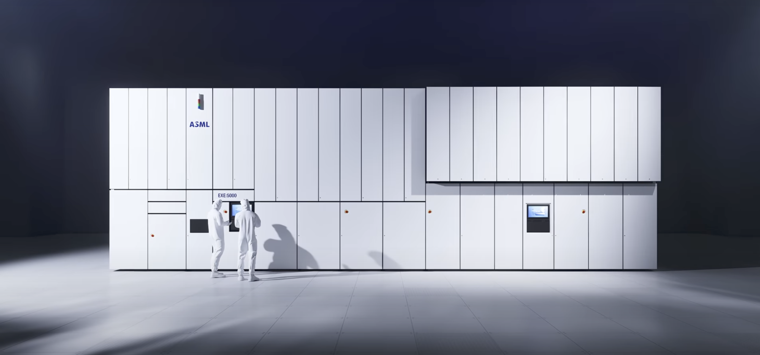
Unlocking Next-Gen AI: How ASML’s High-NA EUV Tools Pave the Way for Advanced Chip Innovation
The world of artificial intelligence is on the cusp of a revolution, and the key to unlocking its full potential lies in the cutting-edge advancements of semiconductor technology. Recently, ASML, a powerhouse in extreme ultraviolet lithography, announced that its new High-NA EUV machines are primed for mass production. This pivotal announcement has sent ripples through the tech industry, signaling that a new era for AI chips is just around the corner.
Why This Matters for AI
The landscape of AI chip production is shifting dramatically. Existing EUV machines have pushed the limits of what’s possible, but they’ve hit a ceiling. This is where the High-NA EUV tools come into play. They promise to redefine chip manufacturing by enabling the creation of finer and more densely packed circuit patterns with increased efficiency.
“As we assess the learning cycles amassed through extensive customer testing, it’s evident we are at a critical juncture,” noted Marco Pieters, ASML’s Chief Technology Officer, in an exclusive interview with Reuters.
The Numbers That Matter
ASML’s declaration of readiness isn’t just hot air; it’s backed by compelling data. The High-NA EUV tools have achieved significant milestones:
- 500,000 silicon wafers processed
- Approximately 80% uptime, with aspirations to reach 90% by year-end
- Imaging precision that simplifies the chip fabrication process, replacing multiple steps with a single High-NA pass
Pieters highlighted that these metrics indicate the tools are poised for manufacturer qualification. However, they come with a hefty price tag—around $400 million per unit, making them among the priciest industrial equipment available today. Early adopters like TSMC and Intel are already on board, eagerly incorporating this innovative technology.
A Two-to-Three-Year Runway
While the technical aspects are ready to go, integration into existing high-volume production lines will take time. Pieters emphasized the distinction between readiness and manufacturing integration. It’s anticipated that this process will span two to three years as chipmakers navigate qualification and refine development processes.
“Chipmakers have accumulated the expertise necessary to qualify these tools,” he stated. This sentiment reflects confidence in the industry’s capabilities, even as they face a measured timeline.
For those in the AI sector, the next wave of chip performance enhancements is on the horizon, almost within reach. ASML’s announcement marks the beginning of an exhilarating race to integrate High-NA EUV technology into mainstream production.
As we stand on the threshold of this groundbreaking leap in technology, the future of AI is brighter than ever. Embrace the unfolding journey towards unparalleled advancements in semiconductor capabilities—stay informed and inspired!